Introduction
This page details the work I undertook when developing an AVR-based Satellite system. This system is no longer in development, as I have since moved on to developing an Atmel ARM-based solution (click here for more). If you are interested in the Epilogue of this system, skip to the end. Otherwise, if you are interested in my older system, read on. Most of what follows is in its original form as written at the time.
Original Introduction
The Satellite system provides a means for a Raspberry Pi to work with and control multiple AVR-based satellites. The Pi drives the complete system, with the satellites providing timing-critical functionality that the Pi has some difficulty providing on its own. Each satellite can be located either locally (ie. right next to the Pi) or at a distance.
Each satellite is driven by an AVR microcontroller and a number of other useful ICs, depending on the design. The following designs are provided at the moment:
- The Vanilla design provides a simple, minimalist layout, using an ATmega328 and a small number of optional components.
- The Chocolate design is more complex, but highly customisable, and has considerably more features. It provides sixteen high current (150mA) outputs, eleven signal outputs, three hardware PWM outputs, seven inputs, and eight ADC lines for sensors. It can be built using readily available components.
A bus design is also provided to allow the AVR MCUs to operate at 5V without harming the Raspberry Pi's voltage-sensitive inputs. This allows you to run the AVR at full speed with 5V power, enabling speeds up to 20MHz, without risking damage to your Pi.
The combination of a Raspberry Pi and AVR microcontrollers works extremely well, with the strengths of each covering the weaknesses of the other. For example: The Pi runs a complete operating system with considerable hardware support, and has plenty of memory, processing, and storage available for use. The AVR MCUs are ideal for timing-sensitive outputs and sensors. They provide multiple hardware PWM outputs, and are fast and precise enough to perform reasonable quality software PWM on multiple outputs. They provide 10-bit ADC across multiple inputs. They are also priced very reasonably- about $5-$7 each.
Satellite (Vanilla)
Schematic
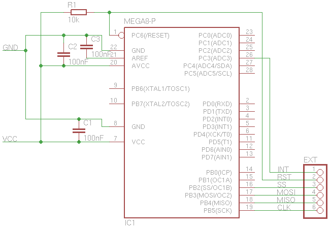
Design Notes
The Vanilla is a simple, minimal Satellite design. It is a good choice when starting with the Satellite system.
Details:
- Each of the included components are recommended, but can be left out if you do not have them on hand (see below for the consequences).
Using a Raspberry Pi:
- The CLK, MOSI, and MISO lines should be connected as follows: CLK to GPIO11(SPI_CLK), MOSI to GPIO10(SPI_MOSI), and MISO to GPIO09(SPI_MISO).
- The SS line should be connected to GPIO8(SPI_CE0_N), but you can choose to use another pin.
- RST and INT lines should be connected to two GPIO pins of your choice on the Pi.
- VCC should be connected to one of the 3.3V power pins on the Pi. Do not connect it to the 5V pins as this will result in damage to your Pi.
- GND should be connected to one of the GND pins on the Pi.
Some possible changes in this design:
- Resistor R1 can be left out if unavailable. This may cause the MCU to spontaneously reset in noisy electronic environments.
- Capacitor C1 can be left out if unavailable. This may cause the MCU to misbehave or fail in noisy electronic environments.
- Capacitor C2 can be left out if unavailable. This will mean the analog inputs will considerably be less accurate.
- Capacitor C3 can be left out if unavailable. This will mean that you cannot use analog input reliably.
- You can add an external crystal or oscillator on XTAL1 and XTAL2 if you want to go faster than the default 8MHz or want a more accurate clock. However, you will be unable to go above 12MHz due to using 3.3V power.
Bus
Schematic
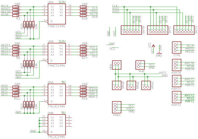
Design Notes
This is an updated bus design based on my original design, but using more suitable ICs. It uses a SN74HCT244N and a SN74LVC244N. Up to three Satellites are supported with this design. It can be expanded for more Satellites easily enough by adding more SN74HCT244N and SN74LVC244N ICs.
A SN74HCT244N is used for up-conversion. The SN74HCT244N buffer IC runs at 5V, with the 3.3V-logic-capable inputs accepting signals from the 3.3V side. The signals are output at 5V level on the Satellite side.
A SN74LVC244N is used for down-conversion. The SN74LVC244N buffer IC runs at 3.3V, with the 5V-tolerant inputs accepting signals at 5V. The signals are output at 3.3V level on the Pi side.
There are a number of 100ohm resistors in use in this design. The ones heading back to the Pi (eg. AMISO, AINT0, AINT1) are included as a means to protect against accidental short-circuits. The ones leading to the Satellites are used as a means of reducing noise on those lines.
My goal is to produce a general-purpose solution that works with a variety of distances. For a satellite placed at the end of a 3m RJ45 cable, these resistors were essential to reliably communicate with it. Having said that, one piece of feedback that I have received on this particular design is that it will not provide a reliable, general-purpose trouble-free solution over range. A better solution for this scenario is something along the lines of RS-485, probably with dedicated ICs managing the communication. This would also have the advantage of allowing communication over considerably longer distances.
RSEL is used to select between default HIGH and default LOW for the RST* lines heading to the Satellites. This allows the Satellites to be disabled, which is helpful after making major changes to the circuit layout, before flashing a new image to the MCU.
Old/Cheap Bus
Schematic
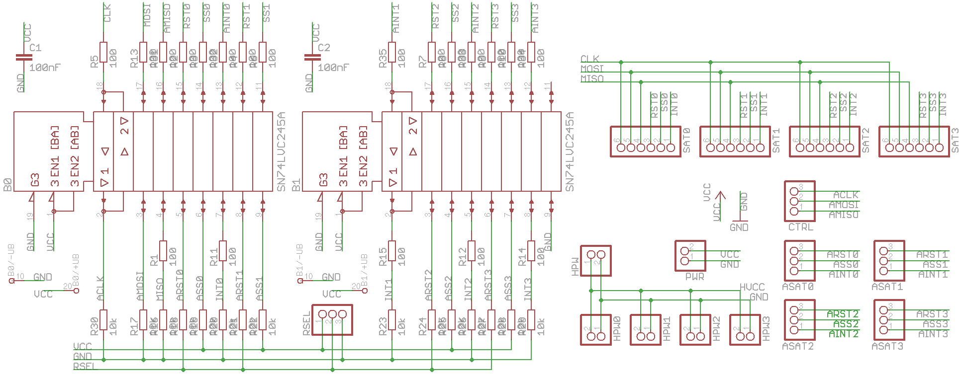
Design Notes
This was my temporary bus design until I located more suitable ICs. Whilst it worked for me, and might do for you, using the SN74LVC245A for up-converting is awfully close to being out-of-spec. I was able to get hold of a lot of SN74LVC245A ICs very cheaply, which made this design very appealing originally.
B0 and B1 provide a separation between the Pi-side environment (3.3V) and the satellite-side (5V).
There are three lines shared between the satellites (SPI CLK, MOSI, MISO), and three lines per satellite (reset, interrupt, and SPI SS). This means that two chips are needed for 2-4 satellites.
The two weaknesses of the design are: (i) the 3.3V Satellite-side outputs are read correctly, but it is quite marginal; and (ii) the 245 series takes a direction signal, which is quite useless and has the potential for issues on startup.
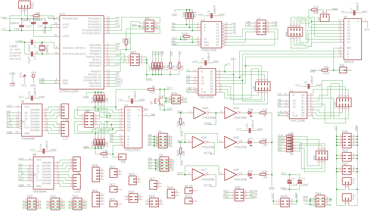
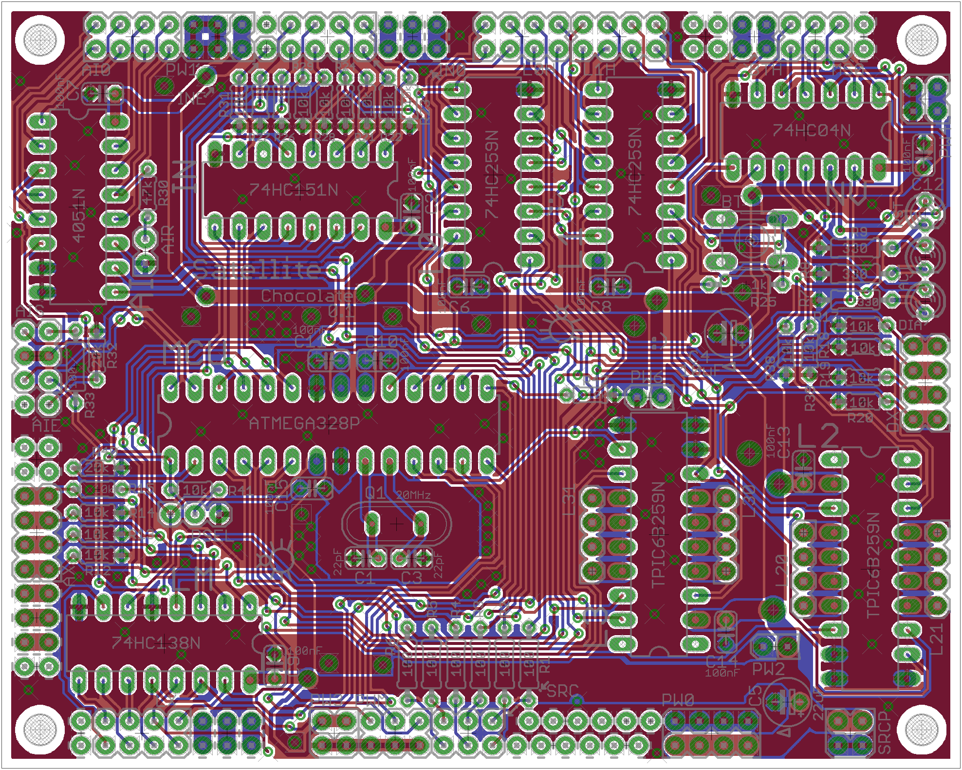
Satellite (Chocolate)
Schematic
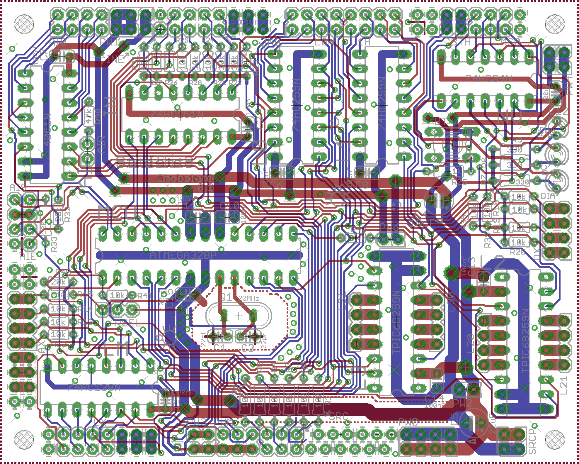
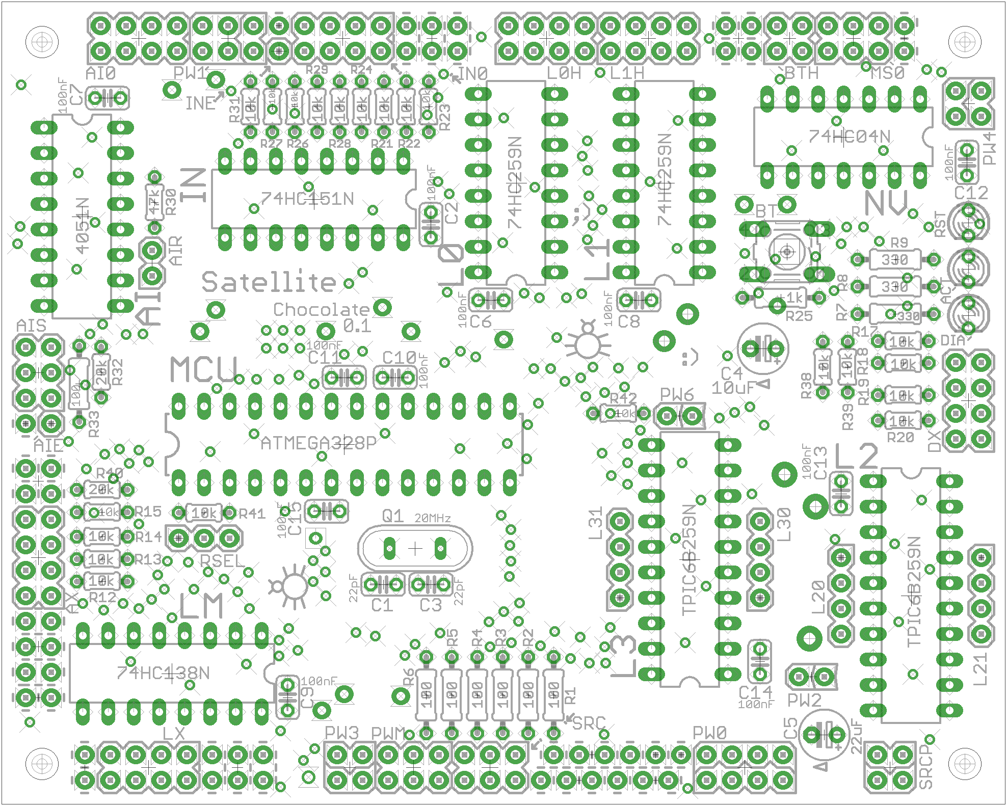
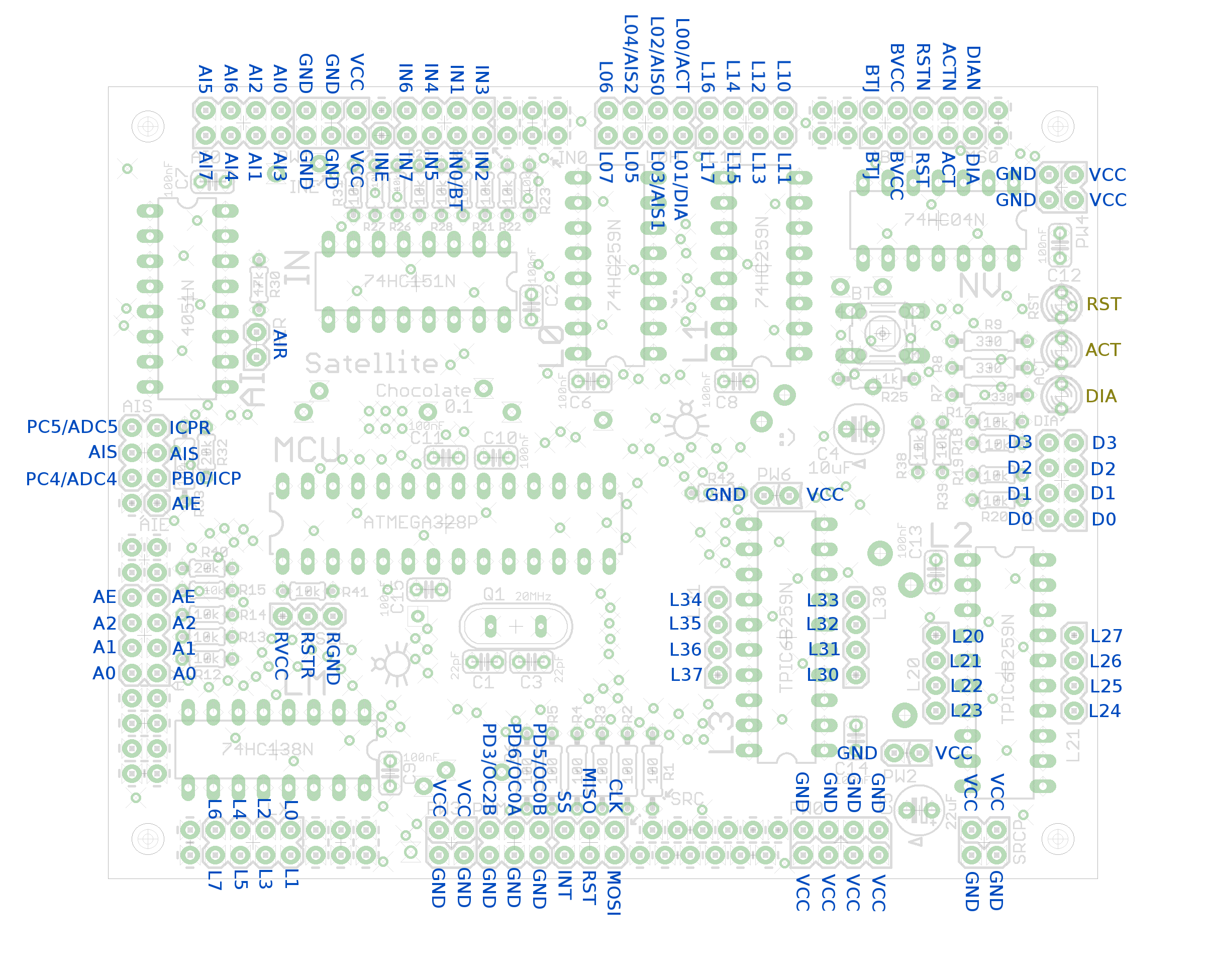
PCB
Complete
No Ground Pour
Silkscreen and Misc
Pin Layout
Gerbers
Design Notes
The aim of this satellite design is to provide a flexible design that can be assembled, customised, and used by someone with very basic computing and electronics ability.
The components used in the design are inexpensive and readily available from multiple manufacturers. The design is such that components can be left out if the functionality provided is not needed, and added back in again later when needed. It is best to think of the completed design presented as one including all of the possible optional extras.
Expansion capability is also provided so that additional desired functionality can be added to an existing system.
The design uses through-hole components with a standard minimum pin distance of 0.1" (2.54mm) between pins.
Features
The default unmodified layout provides the following capabilities:
- 16 high-current outputs (open drain, 150mA/ea, 500mA per each two chips), which can be driven through software PWM.
- 11 low-current output signal lines, ideal for driving other devices. These outputs can also be used for a limited number of LEDs, but you need to watch the current requirements of these devices.
- 7 input lines, plus one on-board button with an external header.
- 8 analog/input-capture inputs, 10-bit ADC, configurable by jumpers.
- 3 hardware PWM outputs or general GPIO pins.
- 0-3 extra GPIO pins, depending on configuration. Two of these are capable of ADC, and one capable of input capture.
- Expansion headers for four further addressable ICs.
- The ability to adjust the design to reduce build cost or gain additional inputs and outputs.
System Overview
The heart of the system is an ATmega328P MCU (listed as "MEGA8-P" on the schematic).
The system is connected via a data bus with four outputs (D0..3), and one input (INI). A set of three address lines (A0..2) plus one enable line (AE) control the currently active component.
LM is a 74HC138 demultiplexer controlled with lines A0..2. Output is active-low. The output lines (L*E) tend to enable/select/activate a single chip, which will then use the four data lines (D0..3) however they wish. The LE line is used to control the output of the selected line (when LE is LOW, the selected line will be LOW). Before switching addresses LE is always brought HIGH.
IN is a eight-input 74HC151 multiplexer controlled with lines A0..2 (the same lines as used by LM). The mux output is INI, which is the single input line used by the MCU. Input 0 is hardcoded to an on-board button, with header BT0 allowing an external button to be added behind the resistor.
L0 and L1 are addressable latches (74HC259). They are controlled by the four data lines (D0..3). Each provides eight low-current outputs suitable for signalling.
L0 has five outputs hardcoded:
- 0: An activity line (ACT) that is pulled low initially, but driven high when the MCU is ready and running code.
- 1: A diagnostic line (DIAG) that is connected to a LED that lights based on code running in the MCU.
- 2-4: These outputs select one of eight analog inputs (see the entry on "AI" below).
L1 is general purpose and has no hardcoded outputs. L0 provides three general purpose outputs, and L1 provides eight. This gives us a total of eleven low-current signal outputs.
L2 and L3 are high power addressable latches (TPIC6B259), and together provide a total of sixteen high-current (150mA per output, 500mA per chip) outputs. None of these outputs are hardcoded and all can be used. These ICs are a little more expensive than the others and can be left out if they are not needed.
The remaining four addresses (enabled by L4..7) are available for custom expansion, and the AX*, DX*, and YX* headers are provided for future expansion.
AI is an analog mux/demux (4051N) that is used to switch between eight analog inputs. The resultant analog input selected can be switched between a combination of the ADC4,ADC5, and PB0 pins, allowing the use of both analog input and input capture. The particular configuration is chosen through jumper selection between the SLR, SLA, and SLD headers. The AIR header is used to pull down signal 0, and should be removed if this is not needed.
NV is a hex inverter (74HC04) and is used to swap various signals and isolate the three board-mounted LEDs.
The PWM header is connected to the three hardware PWM channels that are available in this design, although they can be used for any purpose.
Pin choices for the data lines on the ATmega have been chosen such that TXD and XCK are among the outputs, and RXD is the input line. This should in theory allow hardware SPI via the USART, although my current implementation just bit-bangs it.
There are three status lines, which are also connected to a single on-board LED each:
- The diagnostic line (DIAG): This is controlled entirely through software and is used to indicate the boot sequence and errors. It defaults to LOW. The LED is wired such that it will be on when DIAG is bought HIGH.
- The activity line (ACT): This is brought HIGH by the software once it is running, and defaults to LOW otherwise. The attached LED will be on when ACT is low, ie. if the MCU has not booted or is not running. It will be off once the MCU has booted and is running.
- The reset line (RST): This is directly connected to the MCU's reset pin. A HIGH reset means that the MCU is allowed to run, and LOW disables it. RST is also used when programming (flashing) the MCU. The attached LED will be on when RST is low, ie. when the MCU is being disabled by a LOW signal. It will be off when the MCU is enabled.
Using the LEDs, the boot sequence is as follows:
- Initially ACT and RST will be on.
- If the MCU has been enabled by the RST line, the RST LED will turn off. If the MCU has been disabled by the RST line (deliberately or not), then RST will remain on and nothing will happen.
- If the software on the MCU is running correctly, the ACT LED should turn off. If it does not, the software on the MCU may not be working.
- The diagnostic LED should then blink three times once the MCU has initialised. This is generally the indication that the system is ready to use.
During a MCU reset, some of the initial steps may occur too fast for the eye to see. For example, on a working system you may never see the ACT and RST LEDs turn on. If they turn on and remain on, there may be an issue.
Breadboard Assembly
If you are using breadboards (recommended if you want to experiment with the design) then you will need at least two full-size breadboards, with three recommended. The base design will take up almost two full breadboards if you cram it in, or more if you allow yourself some breathing room. It is possible to trim the design back (ie. leave out some components) to regain space, but this may be difficult if you are not already familiar with the design.
Expansion
Some possible uses for the four expansion addresses provided by the LM IC:
- An addressable latch, either signal or open drain, giving eight more outputs per address used.
- Another analog mux/demux, giving eight more analog or input-capture inputs.
- A bus IC (eg. SN74HC245N) for performing four-way parallel updates of a WS2811 addressable LEDs.
- Chains of shift registers of arbitrary length, allowing effectively unlimited, but slow, output expansion.
The following is also possible, but you will need the software and to write a driver for it:
- Any SPI device. For example, one MCP23S17 could be used to add sixteen GPIO per address to the system.
- Any IC that can be driven by an active-low enable line, four output lines, and one input line (ie. the IC requires less than four inputs and no more than one output).
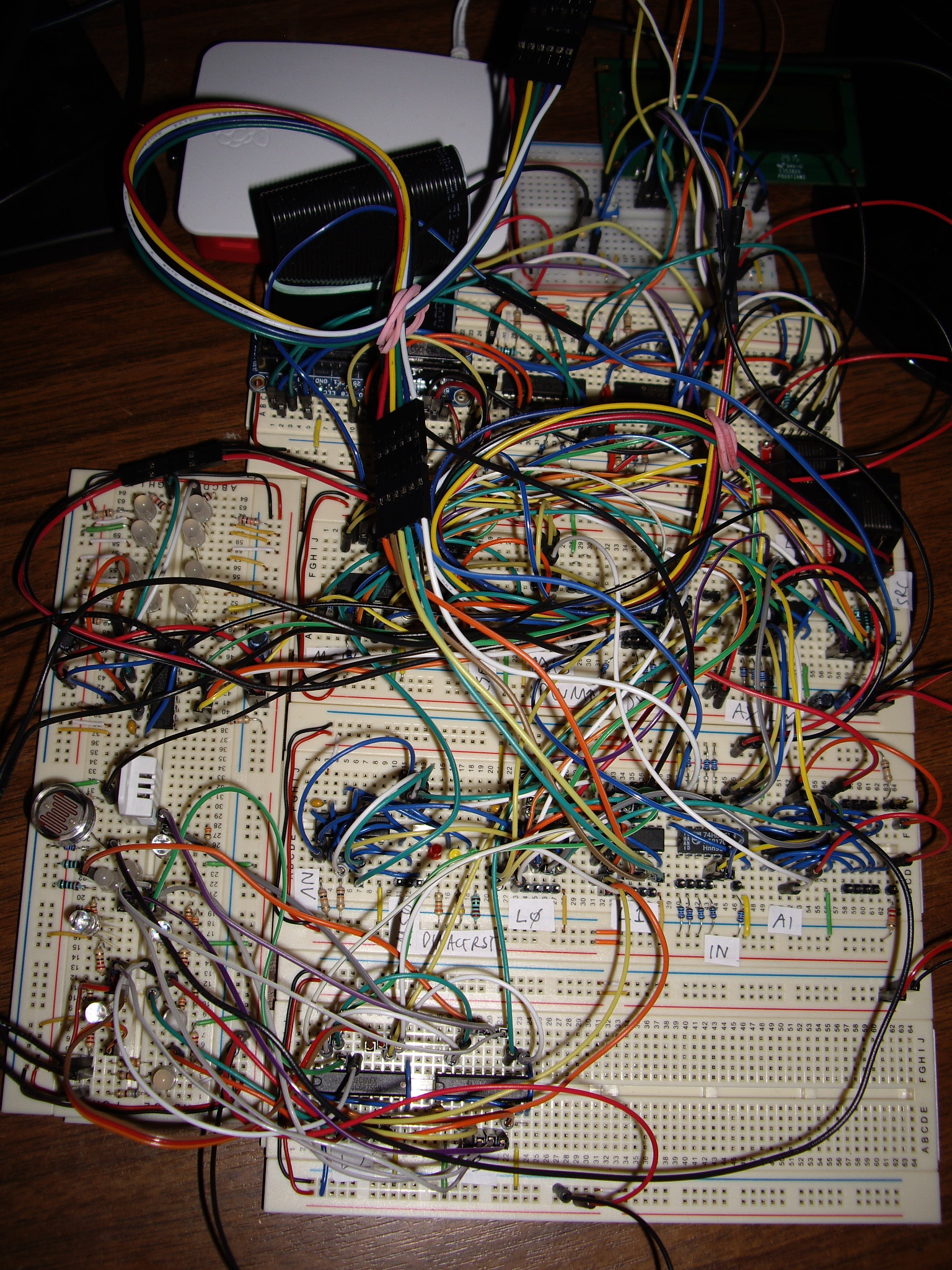
Breadboard Prototype
Following are some images of a full rebuild of a breadboard prototype of the chocolate design directly from the schematic. Note that this build was done to confirm correct test and operation as per the schematic, and is not space-efficient.
The result is here:
Here is a zoomed-in view of the top part of the layout, which is a bit hard to see from the first picture:
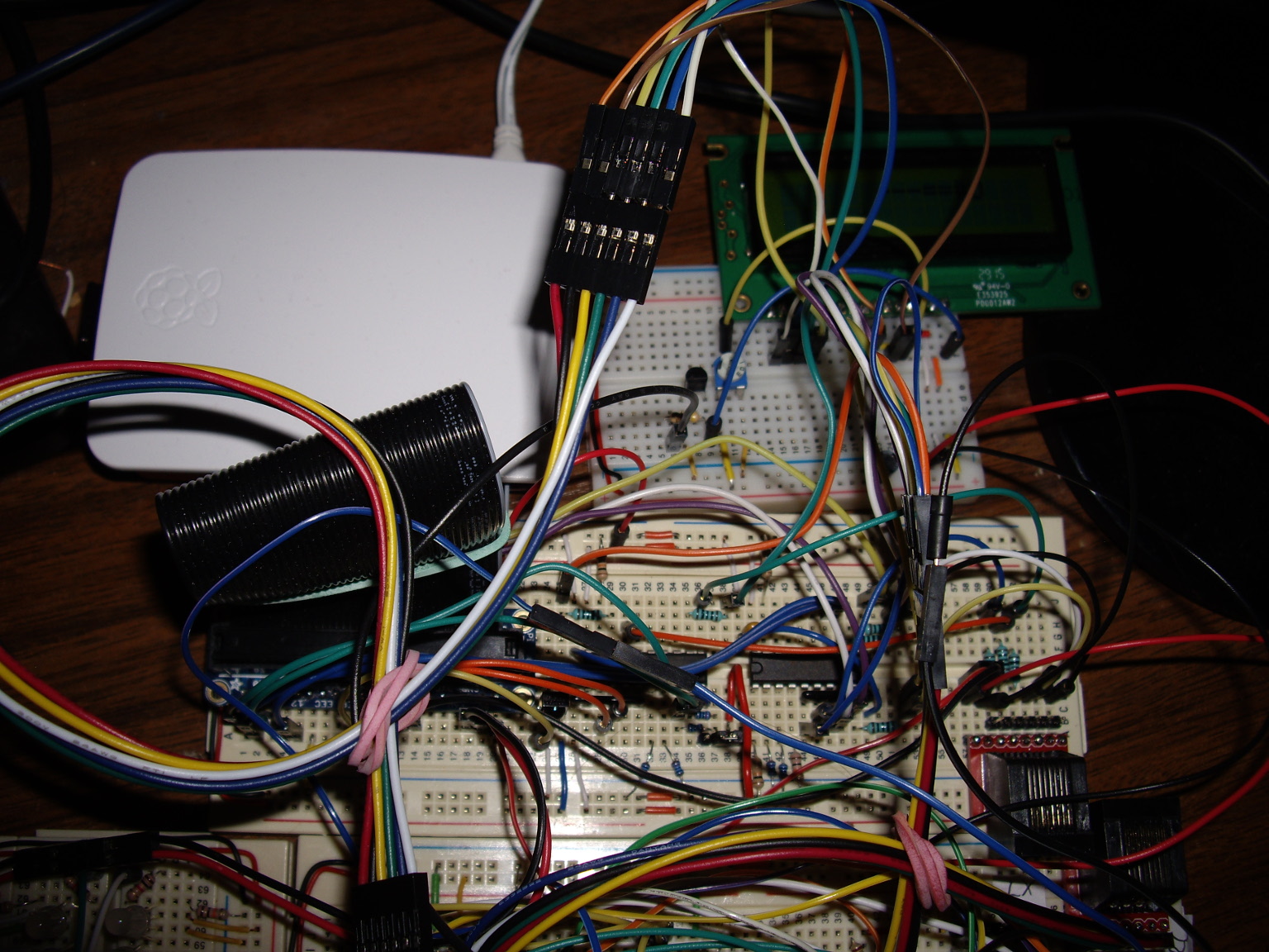
The Pi is at the top left of the main image. Immediately to the right is a half-sized breadboard with the LCD display and some related components. Down from that is the bus board, which contains the Pi breakout, the bus IC, an IR sensor, and an RJ45 socket with breakout.
The three boards in the bottom right of the main image are the rebuild of the chocolate design.
The upper board contains MCU (ATmega328P), and LM (the demux), the bus resistors, and a bunch of headers. The lower board contains L2 and L3 (the TPIC ICs). The central board contains the remaining ICs.
Off to the left is a board with miscellaneous lights and sensors, as the chocolate design is a bit dull without. :) A single RGB LED is controlled via the PWM header. Five other RGB LEDs are controlled through the L2 and L3 outputs (that's 15 channels all up), with two single-colour LEDs controlled by the remaining output. The single IC is a SN74HC245N, which is enabled by an output from LM. The four data lines are used to perform a four-way parallel update of the eight WS2811-based RGB LEDs attached to it. When using an actual chocolate PCB, this particular board would be added using one of the LX pins for an address line, and the DX pins for the four signal lines.
The LCD at the top right is controlled by seven of the eight outputs provided by L1. The first six outputs control the HD44780-compatible LCD, whilst the last output enables a transistor that controls the LCD backlight LED.
The particular components hooked up to the chocolate design mimic those that I plan to use for a personal project that uses the chocolate design as a base.
Arrival of the PCB
I have now the first version of the Chocolate PCB! Here it is:
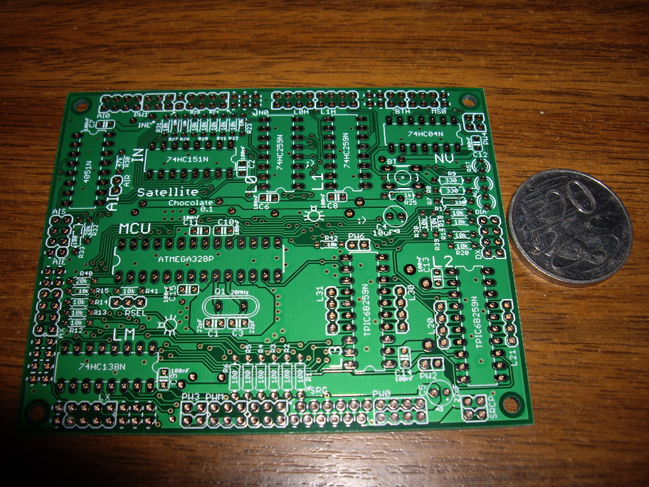
Beautiful isn't it? :)
Here is my prototyping layout with the three breadboards for the Chocolate design replaced with a fully-populated Chocolate PCB:
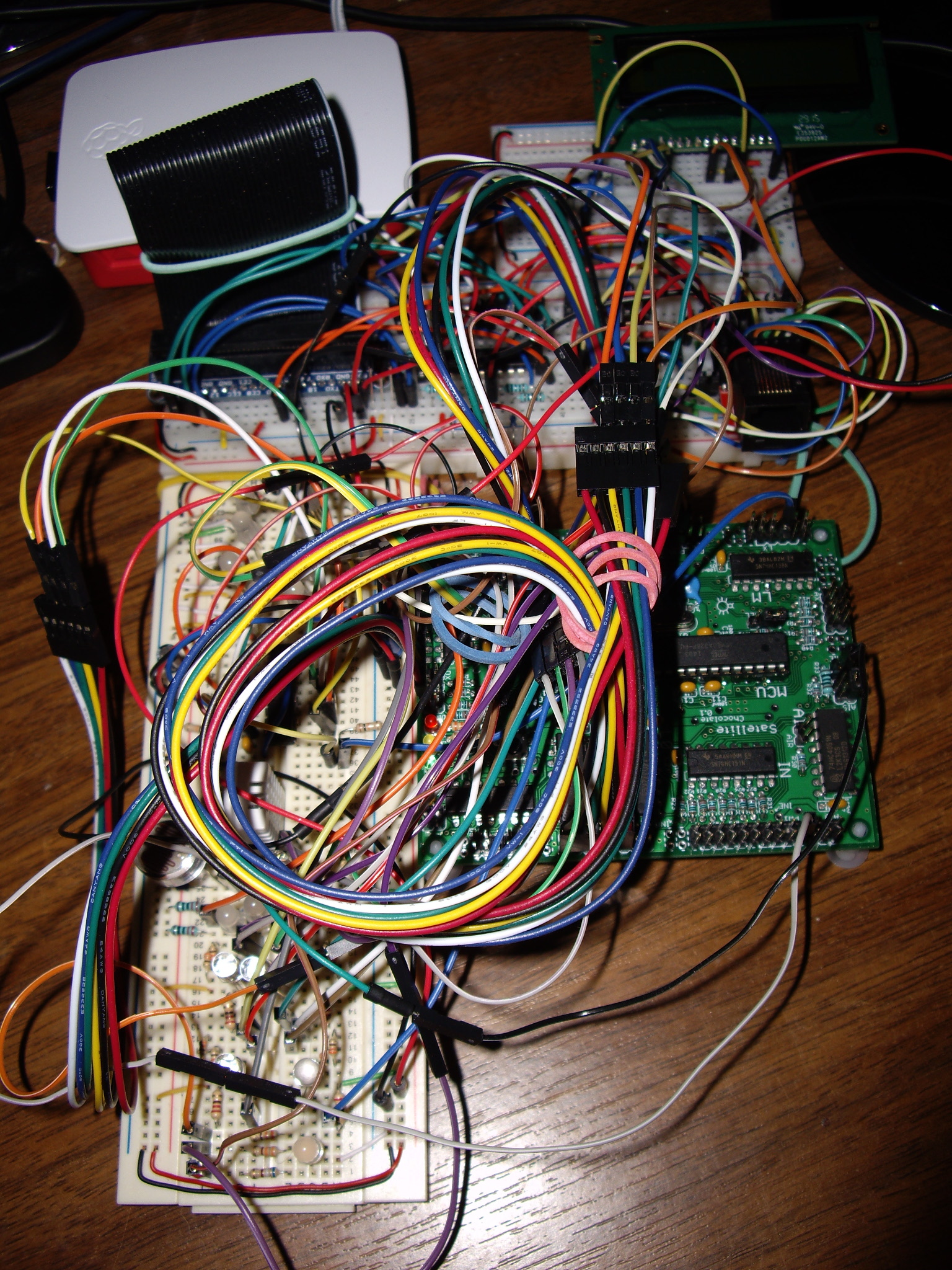
Compare to the breadboard-only prototype above. Much nicer.
In case you are wondering what happened to the bus board- it has been updated to use the newer design. This should ensure that the signal levels are correct.
Here's a closer look at the populated board:
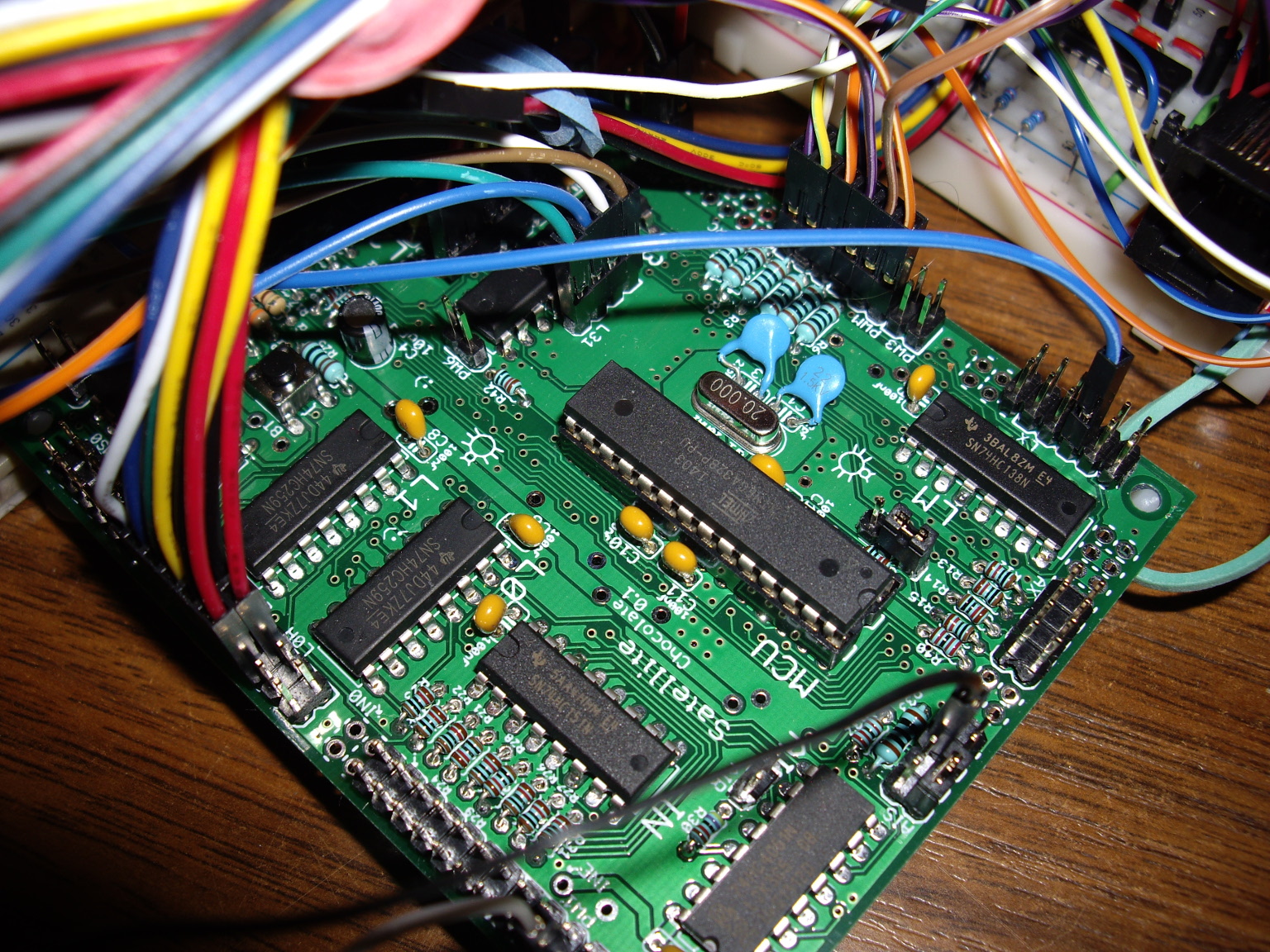
I'm pretty happy with how this has turned out.
Epilogue
The epilogue to the AVR Satellite board can be found here. The successor to this board design can be found here.